- 您现在的位置:买卖IC网 > Sheet目录1214 > EVAL-ADE7878EBZ (Analog Devices Inc)BOARD EVAL FOR ADE7878
�� �
�
�ADE7854/ADE7858/ADE7868/ADE7878�
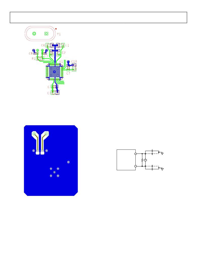
�Figure� 96.� ADE7878� Top� Layer� Printed� Circuit� Board�
�The� exposed� pad� of� the� ADE7878� is� soldered� to� an� equivalent�
�pad� on� the� PCB.� The� AGND� and� DGND� traces� of� the� ADE7878�
�are� then� routed� directly� into� the� PCB� pad.�
�The� bottom� layer� is� composed� mainly� of� a� ground� plane�
�surrounding� as� much� as� possible� the� crystal� traces.�
�Data� Sheet�
�shown� in� Figure� 98.� CL� 1� and� CL� 2� denote� the� capacitances� of� the�
�ceramic� capacitors� attached� to� the� crystal� pins,� whereas� CP� 1� and�
�CP� 2� denote� the� parasitic� capacitances� on� those� pins.�
�The� recommended� typical� value� of� total� capacitance� at� each�
�clock� pin,� CLKIN� and� CLKOUT,� is� 24� pF,� which� means� that�
�Total� Capacitance� =� CP� 1� +� CL� 1� =� CP� 2� +� CL� 2� =� 24� pF�
�Crystal� manufacturer� data� sheets� specify� the� load� capacitance�
�value.� A� total� capacitance� of� 24� pF,� per� clock� pin,� is� recommended;�
�therefore,� select� a� crystal� with� a� 12� pF� load� capacitance.� In�
�addition,� when� selecting� the� ceramic� capacitors,� CL� 1� and� CL� 2� ,�
�the� parasitic� capacitances,� CP� 1� and� CP� 2� ,� on� the� crystal� pins� of�
�the� IC� must� be� taken� into� account.� Thus,� the� values� of� CL� 1� and�
�CL� 2� must� be� based� on� the� following� expression:�
�CL� 1� =� CL� 2� =� 2� � Crystal� Load� Capacitance� ?� CP� 1�
�where� CP� 1� =� CP� 2� .�
�For� example,� if� a� 12� pF� crystal� is� chosen� and� the� parasitic�
�capacitances� on� the� clock� pins� are� CP� 1� =� CP� 2� =� 2� pF,� the� ceramic�
�capacitors� that� must� be� used� in� the� crystal� circuit� are� CL� 1� =� CL� 2�
�=� 22� pF.�
�The� Evaluation� Board� EVAL-ADE7878EBZ� uses� the� crystal�
�VM6-1D11C12-TR-16.384MHZ� (maximum� drive� level� 1� mW;�
�maximum� ESR� 20� Ω;� load� capacitance� 12� pF).� It� is� recommended�
�that� the� same� crystal,� or� a� crystal� with� similar� specifications,� be�
�selected.� Lower� values� of� ESR� and� load� capacitance� and� higher�
�values� of� drive� level� capability� of� the� crystal� are� preferable.�
�It� is� also� recommended� that� a� 5� M� resistor� be� attached� in�
��CL� 2�
�CLKIN�
�CP� 2�
�GND�
�ADE78xx� IC�
�5M� ?�
�16.384MHz� CRYSTAL�
�CP� 1�
�CLKOUT�
�GND�
�CL� 1�
�Figure� 98.� Crystal� Circuit�
�ADE7878� EVALUATION� BOARD�
�An� evaluation� board� built� upon� the� ADE7878� configuration�
�supports� all� ADE7854� ,� ADE7858� ,� ADE7868� ,� and� ADE7878�
�components.� Visit� www.analog.com/ADE7878� for� details.�
�Figure� 97.� ADE7878� Bottom� Layer� Printed� Circuit� Board�
�DIE� VERSION�
�CRYSTAL� CIRCUIT�
�The� register� named� version� identifies� the� version� of� the� die.� It� is�
�an� 8-bit,� read-only� version� register� located� at� Address� 0xE707.�
�A� digital� clock� signal� of� 16.384� MHz� can� be� provided� to� the�
��Alternatively,� attach� a� crystal� of� the� specified� frequency,� as�
�Rev.� H� |� Page� 76� of� 100�
�发布紧急采购,3分钟左右您将得到回复。
相关PDF资料
EVAL-ADE7880EBZ
BOARD EVAL FOR ADE7880
EVAL-ADE7953EBZ
BOARD EVAL FOR ADE7953
EVAL-ADF4002EBZ1
BOARD EVAL FOR ADF4002
EVAL-ADG788EBZ
BOARD EVALUATION FOR ADG788
EVAL-ADM1021AEB
BOARD EVAL FOR ADM1021
EVAL-ADM1023EB
BOARD EVAL FOR ADM1023
EVAL-ADM1031EB
BOARD EVAL FOR ADM1031
EVAL-ADM1062TQEBZ
BOARD EVALUATION FOR ADM1062TQ
相关代理商/技术参数
EVAL-ADE7880EBZ
功能描述:BOARD EVAL FOR ADE7880 RoHS:是 类别:编程器,开发系统 >> 评估演示板和套件 系列:* 产品培训模块:Obsolescence Mitigation Program 标准包装:1 系列:- 主要目的:电源管理,电池充电器 嵌入式:否 已用 IC / 零件:MAX8903A 主要属性:1 芯锂离子电池 次要属性:状态 LED 已供物品:板
EVAL-ADE7880EBZ
制造商:Analog Devices 功能描述:ADE7880, ENERGY METER, 3 PH, SPI, I2C, E
EVAL-ADE7913EBZ
制造商:AD 制造商全称:Analog Devices 功能描述:3-Channel, Isolated, Sigma-Delta ADC with SPI
EVAL-ADE7953EBZ
功能描述:BOARD EVAL FOR ADE7953 RoHS:是 类别:编程器,开发系统 >> 评估演示板和套件 系列:- 标准包装:1 系列:PSoC® 主要目的:电源管理,热管理 嵌入式:- 已用 IC / 零件:- 主要属性:- 次要属性:- 已供物品:板,CD,电源
EVAL-ADF4001EBZ2
制造商:Analog Devices 功能描述:Evaluation Board For Pll Frequency Synthesizer 制造商:Analog Devices 功能描述:ADF4001 PLL SYNTHESIZER EVAL BOARD
EVAL-ADF4002EB1
制造商:Analog Devices 功能描述:EVAL BOARD - Bulk
EVAL-ADF4002EBZ1
功能描述:BOARD EVAL FOR ADF4002 RoHS:是 类别:编程器,开发系统 >> 评估演示板和套件 系列:- 产品培训模块:Obsolescence Mitigation Program 标准包装:1 系列:- 主要目的:电源管理,电池充电器 嵌入式:否 已用 IC / 零件:MAX8903A 主要属性:1 芯锂离子电池 次要属性:状态 LED 已供物品:板
EVAL-ADF4007EBZ1
功能描述:BOARD EVALUATION FOR ADF4007EB1 RoHS:是 类别:编程器,开发系统 >> 评估演示板和套件 系列:- 标准包装:1 系列:PSoC® 主要目的:电源管理,热管理 嵌入式:- 已用 IC / 零件:- 主要属性:- 次要属性:- 已供物品:板,CD,电源